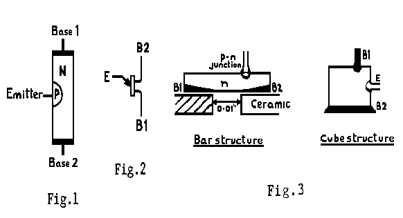
The basic structure of a unijunction transistor (UJT) is shown in
Fig.1. It is essentially a bar of N type semiconductor material into
which P type material has been diffused somewhere along its length.
Contacts are then made to the device as shown; these are referred to as
the emitter, base 1 and base 2 respectively. Fig.2 shows the schematic
symbol used to denote a UJT in circuit diagrams. For ease of
manufacture alternative methods of making contact with the bar have
been developed, giving rise to the two types of structure - bar and
cube - shown in Fig.3 

The equivalent circuit shown in Fig.4 has been developed to explain how
the device works, and it is necessary to define the terms used in this
explanation.
RBB is known as the interbase resistance, and is the sum of RB1 and RB2:
RBB = RB1 + RB2 (1)
N.B. This is only true when the emitter is open circuit.
VRB1 is the voltage developed across RB1; this is given by the voltage divider rule:
RB1
VRB1 = (2)
RB1 + RB2
Since the denominator of equation 2 is equal to equation 1, the former can be rewritten as:
RB1
VRB1 = x VBB (3)
RBB
The ratio RB1 / RBB is referred to as the intrinsic standoff ratio and is denoted by

(the Greek letter eta).
If an external voltage Ve is connected to the emitter, the equivalent circuit can be redrawn as shown in Fig.5.
If Ve is less than VRB1, the diode is reverse biased and the circuit behaves as though the emitter was open circuit. If however Ve is increased so that it exceeds VRB1
by at least 0.7V, the diode becomes forward biased and emitter current
Ie flows into the base 1 region. Because of this, the value of RB1
decreases. It has been suggested that this is due to the presence of
additional charge carriers (holes) in the bar. Further increase in Ve causes the emitter current to increase which in turn reduces RB1 and this causes a further increase in current. This runaway effect is termed regeneration. The value of emitter voltage at which this occurs is known as
the peak voltage VP and is given by: VP =

AVVBB + VD (4)The characteristics of the UJT are illustrated by the graph of emitter voltage against emitter current (Fig.6).


As the emitter voltage is increased, the current is very small - just a
few microamps. When the peak point is reached, the current rises
rapidly, until at the valley point the device runs into saturation. At
this point RB1 is at its lowest value, which is known as the saturation resistance.
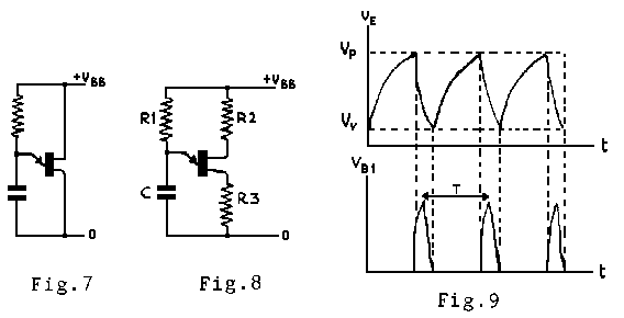
The simplest application of a UJT is as a relaxation oscillator,
which is defined as one in which a capacitor is charged gradually and
then discharged rapidly. The basic circuit is shown in Fig.7; in the
practical circuit of Fig.8 R3 limits the emitter current and provides a
voltage pulse, while R2 provides a measure of temperature compensation.
Fig. 9 shows the waveforms occurring at the emitter and base 1; the
first is an approximation to a sawtooth and the second is a pulse of
short duration.

The operation of the circuit is as follows: C1 charges through R1 until
the voltage across it reaches the peak point. The emitter current then
rises rapidly, discharging C1 through the base 1 region and R3. The
sudden rise of current through R3 produces the voltage pulse. When the
current falls to IV the UJT switches off and the cycle is repeated.
It can be shown that the time t between successive pulses is given by:
VBB - VV
t + R1C ln secs (5) N.B. R measured in Megaohms. C in µF 
